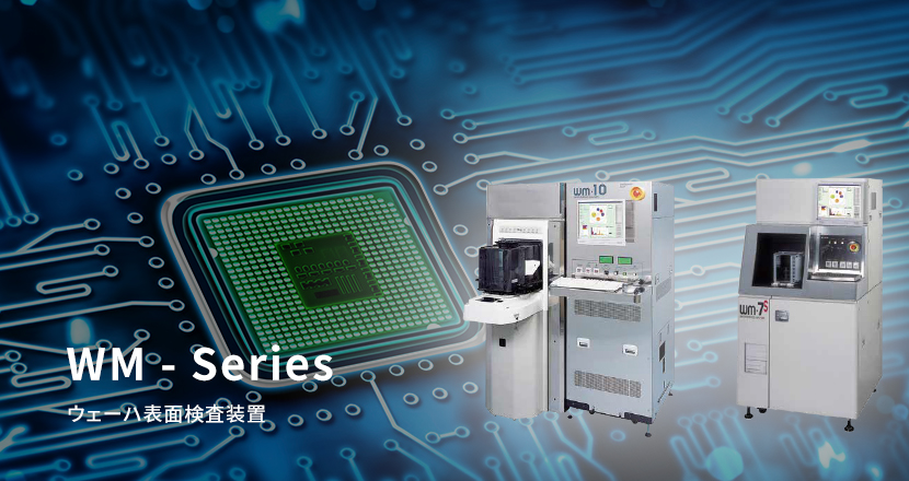
ウェーハ表面検査装置 (WM series)
Thank you for accessing our product page.
We understand you surf the internet a lot to reach here to search particle inspection systems, but no more surf needed.
We Takano offers Non-Patterned 200/300mm wafer surface inspection system.
For your wafer surface inspection requirements.
We understand you surf the internet a lot to reach here to search particle inspection systems, but no more surf needed.
We Takano offers Non-Patterned 200/300mm wafer surface inspection system.
For your wafer surface inspection requirements.
製品情報Product Information ウェーハ表面検査装置 (WM series)
Non-patterned 300mm Wafer surface Inspection system

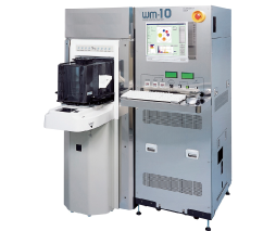
WM – 10 is a standard model of 300 mm wafer.
It is a high sensitivity inspection system of 48 nm.
Non-patterned below 200mm Wafer surface Inspection system

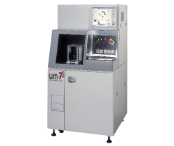
WM – 7 series is the most reasonable high – performance model below 200 mm wafer size.
WM – 7SG can inspect transparent wafers.
WM-series Specification
| WM-10 | WM-7S/7SG | |
|---|---|---|
| Sensitivity | 48nm@Bare-Wafer | 80nm@Bare-wafer:WM-7S 200nm@Glass-wafer:WM-7SG |
| Wafer Size | ~300mm | ~200mm |
| Optical Source | Laser Diode(405nm) | |
| Loader | FOUP(1 or2)/Open Cassette | Open Cassette |
| Size | 1482mm×1173mm×1950mm | 860mm×900mm×1650mm |
| Application | Bare-wafer/Filmed-wafer | |
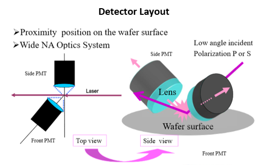
1. Original Optical System for High-sensitivity
- WM-10 have 2axis Incident angle for particle.
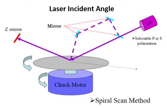
- WM-series have 2 wide NA lens for High-sensitivity detected.
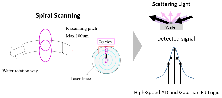
2. Spiral Scan With high-resolution XY-potsion
- WM-series are spiral scan method with rotation speed control.
- XY-Data send to EB review Equipment then it can be review with easy alignment.
お問い合わせ
まずは、下記フォームからお問い合わせください。
お急ぎの方、もしくは、担当者に直接ご相談されたい方は、こちらの番号にお電話ください。
台湾鷹野股份有限公司(桃園事務所)
TEL:03-3413-882